An S-parameter test set emulator: retrofitting off-brand test sets for the HP 8753


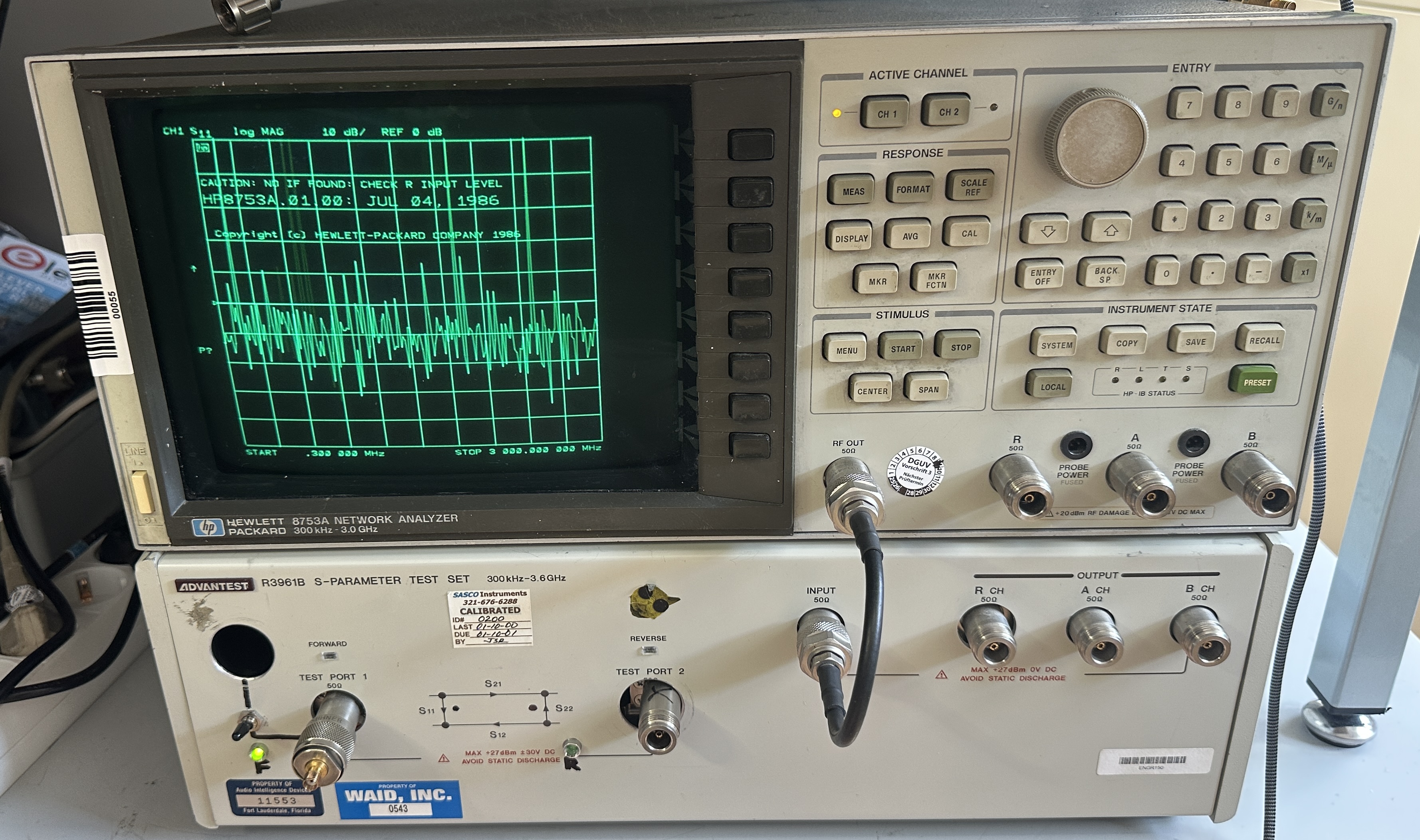
The HP 8753 is probably the most popular vector network analyzer ever built - but the analyzer alone is only half of the instrument. For full two-port S-parameter measurements it wants an S-parameter test set underneath: the 85046A for the 8753A or the 85047A for the 8753B and later. And exactly those boxes still fetch surprisingly serious money on the used market. Meanwhile perfectly fine off-brand test sets - like the Advantest R3961B (300 kHz - 3.6 GHz) in the picture above - can be had for a fraction, simply because they don't speak HP's test set control bus. Inside it's the same story everywhere: a transfer switch, a step attenuator, splitter and bridges. The only thing missing is the handshake. So why not teach the off-brand box to play along? This is the story of a small emulator that makes the 8753 believe it is talking to a genuine 85046A or 85047A while the actual switching happens inside the Advantest.
The test set control bus

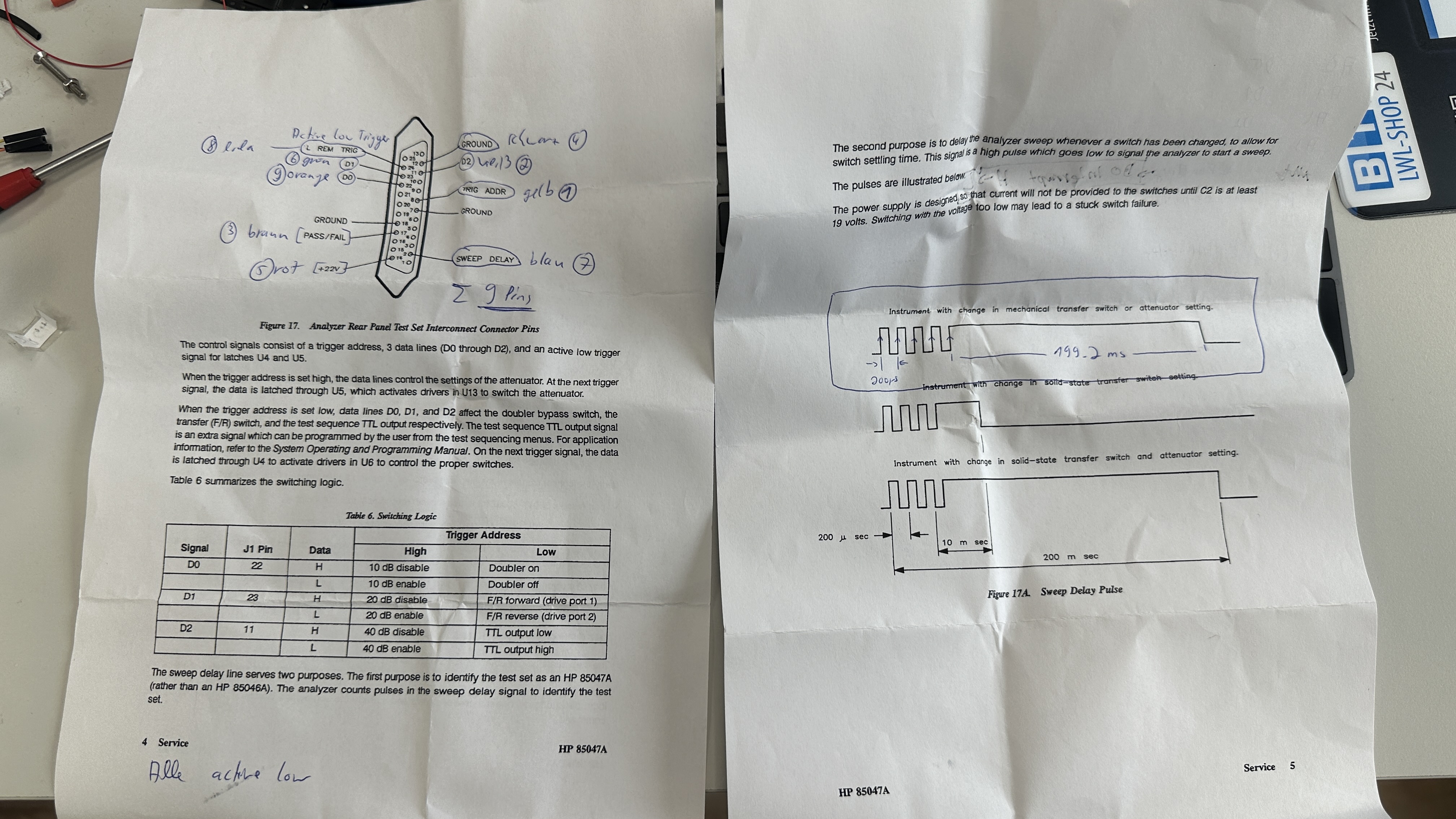
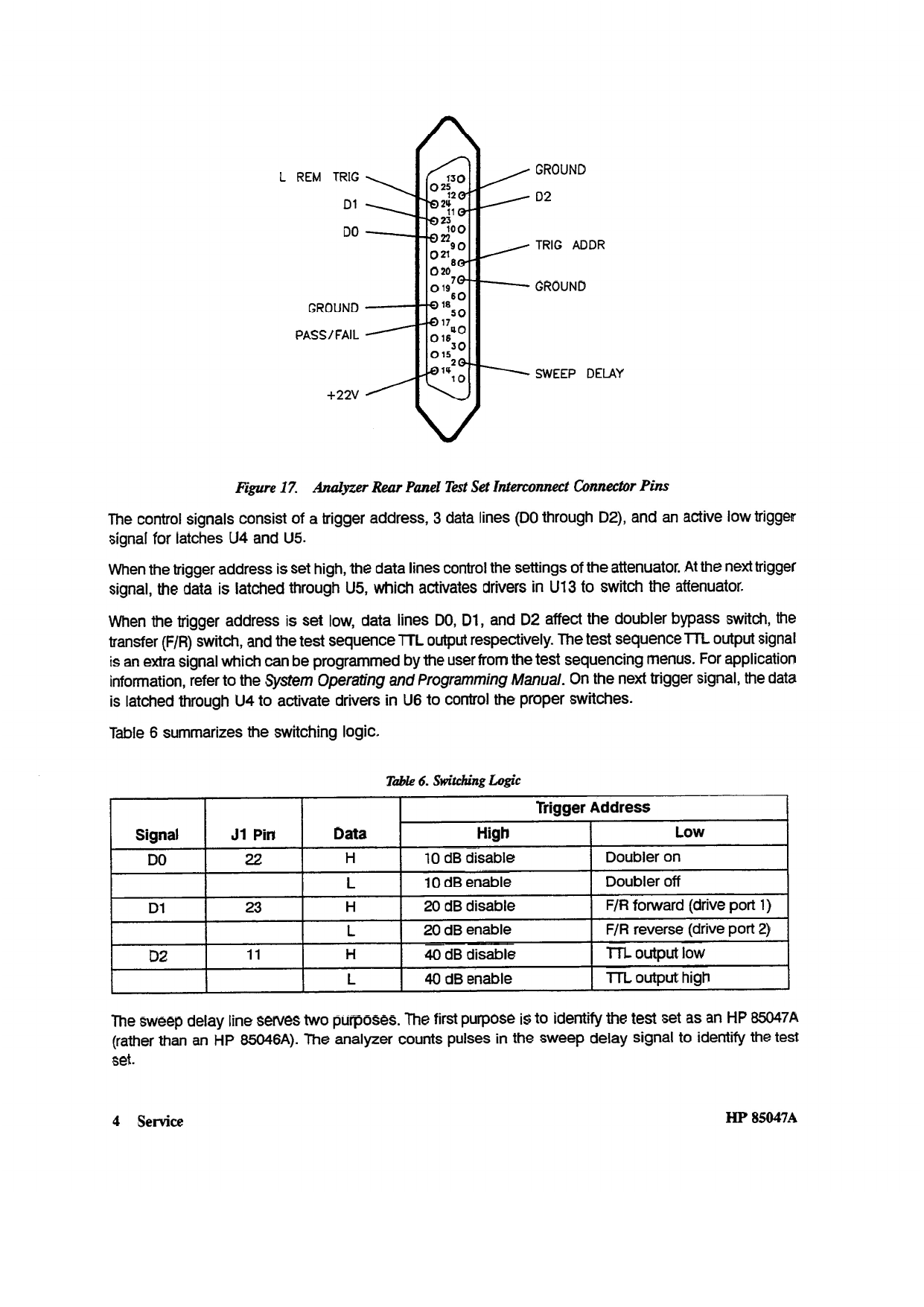
The interconnect between analyzer and test set is a DB25 cable carrying a handful of 5V TTL lines: three data lines, a trigger address line and an active-low trigger strobe from the analyzer, plus one line going back: SWEEP DELAY. On the 85047A the protocol works like two latches (which is exactly what sits in the real test set, U4 and U5): a trigger with TRIG ADDR high latches D0..D2 as the attenuator setting, a trigger with TRIG ADDR low latches the doubler bypass, the transfer (F/R) switch and a user-programmable TTL output. The older 85046A is even simpler - every trigger latches the three attenuator lines and L REM REV directly, no doubler involved.


The 85047A interconnect pins and the switching logic (Table 6) from the service information

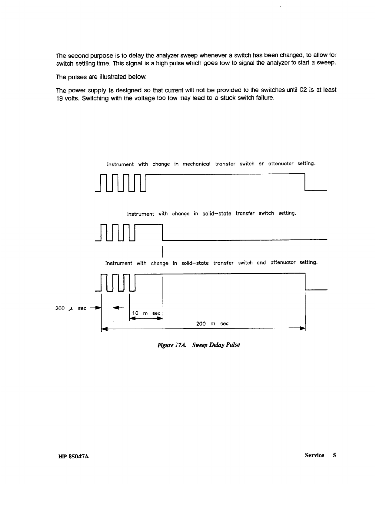
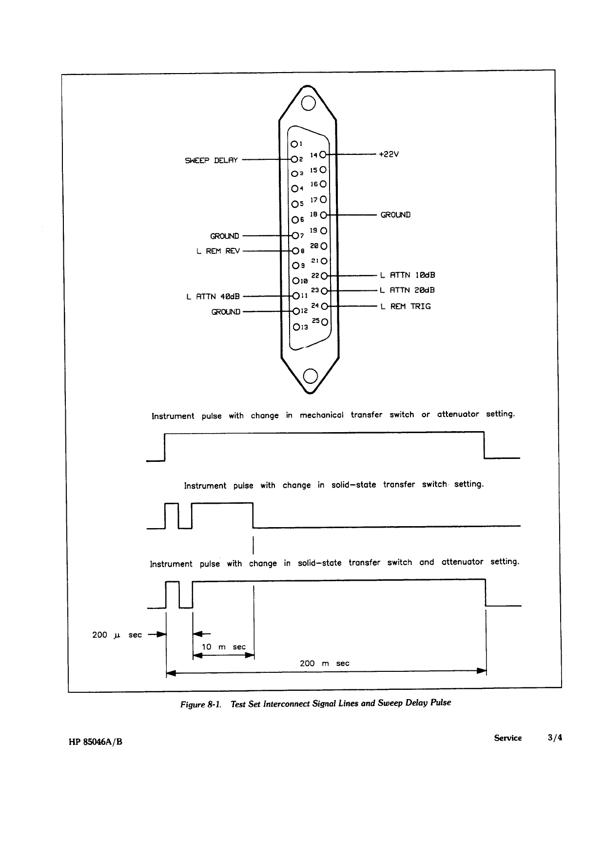
The SWEEP DELAY line is where it gets interesting, as it serves two purposes. First, it identifies the test set: after latching, the test set answers with a burst of identification pulses and the analyzer counts them to tell a 85047A from a 85046A. Second, the line stays high afterwards to hold off the analyzer's sweep until the RF switches have actually settled - a mechanical transfer switch gets a generous 200 ms, the solid-state version only 10 ms. Here are the timing diagrams of both test sets from the HP manuals:

 
Left: 85046A sweep delay pulse (Figure 8-1) - right: 85047A sweep delay pulse with identification pulses (Figure 17A)

Round one, 2016: a PIC16F876A

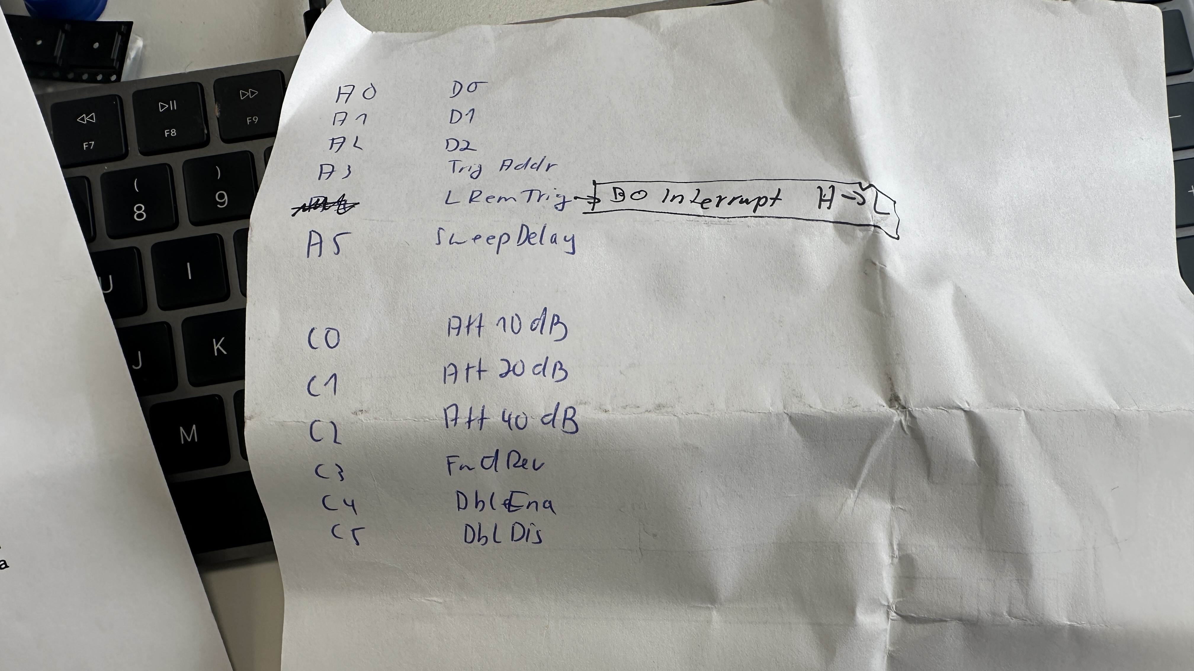
This is actually not a new project. Back in 2016 I retrofitted the R3961B with a little PIC16F876A doing exactly this job: an external interrupt on the falling trigger edge latched the port, and the sweep delay waveform - four identification pulses of 100/100 µs followed by a 199 ms hold - was simply bit-banged with delay loops. The whole reverse engineering happened on paper, with the manual excerpts above on the bench and the wire colors of the adapter cable scribbled next to the connector drawing:

 
The 2016 paperwork: annotated manual pages and the PIC pin mapping

The PIC ran overclocked at 20 MHz and basically raced its interrupt latency against the analyzer's trigger timing - it worked, and it kept working for almost a decade. But it was hardcoded to the 85047A protocol, the timing was frozen in delay loops and there was zero visibility into what was happening on the bus.

Round two: a Pico 2 does it properly

Almost ten years later the trusty PIC got replaced by a Raspberry Pi Pico 2 (RP2350) - not because it was broken, but because I wanted one firmware that can emulate either test set, selectable at runtime, with adjustable timing and a proper debug view of the bus. And the RP2350's PIO blocks are simply made for this kind of job:

. PIO SM0 latches D0..D2 and TRIG ADDR / L REM REV at the falling edge of L REM TRIG, exactly like the edge-triggered latches in the real test sets. It samples at the full 150 MHz system clock - and that is no luxury: the 8753A's trigger pulse turned out to be only 240 ns long (measured with the logic analyzer). The first firmware version had a 0.5 µs deglitch filter on the trigger line which cheerfully rejected every single real pulse :-)
. PIO SM1 + DMA play the complete SWEEP DELAY waveform (identification pulses plus settling hold) with 1 µs resolution, completely unaffected by anything the CPU is doing. A new trigger retriggers the waveform from the start.
. The CPU only decodes the latched transactions, drives the switch outputs (within a few µs - the RF switches themselves take milliseconds anyway) and serves the serial console.

Wiring

The bus lines are 5V TTL; the RP2350 GPIOs are 5V tolerant while powered, so the inputs can connect directly (a ~1k series resistor per line is cheap insurance). The outputs are 3.3V, which satisfies TTL VIH of 2.0V for the analyzer's SWEEP DELAY input - just check that your switch driver stage also accepts 3.3V levels (the PIC drove it with 5V).

The SUB-D9 column below is the bus entry connector on the back panel of the modified R3961B that hosts the emulator; the adapter cable converts the 8753's DB25 interconnect to it. The two HP test sets use identical connector pinouts - TRIG ADDR (85047A) and L REM REV (85046A) are just two names for the same J1 pin 8 - so the adapter built for the PIC back in 2016 connects unchanged. GP2..GP6 must stay contiguous (the PIO samples them as one group); all inputs have their internal pull-ups enabled.

DB25 (J1) SUB-D9 85047A signal 85046A signal Pico 2 Dir
229D0L ATTN 10 dBGP2in
236D1L ATTN 20 dBGP3in
112D2L ATTN 40 dBGP4in
81TRIG ADDRL REM REVGP5in
248L REM TRIGL REM TRIGGP6in
27SWEEP DELAYSWEEP DELAYGP8out
124GNDGNDGND-

The outputs to the switch driver stage are bit-identical in polarity to the old PIC firmware:

Pico 2 Signal Polarity
GP10ATT 10 dBhigh = section disabled (follows bus)
GP11ATT 20 dBhigh = section disabled
GP12ATT 40 dBhigh = section disabled
GP13F/Rlow = forward, high = reverse
GP14Doubler enablehigh = doubler engaged
GP15Doubler disablecomplement of GP14
GP9Test-seq TTL out85047A rear-panel TTL output (new)

The power-up state is all attenuator sections in (70 dB), forward, doubler off - with GP15 actively driven high, where the PIC left both doubler lines low until the first trigger.

Emulation behavior

In 85047A mode a trigger with TRIG ADDR high latches D0..D2 as attenuator disable bits and applies them immediately, exactly as the manual describes it (the PIC used to defer this to the next address-low trigger); a trigger with TRIG ADDR low latches doubler (D0), F/R (D1) and the test sequence TTL output (D2). The sweep delay defaults to 4 identification pulses of 100/100 µs followed by a 200 ms hold.

In 85046A mode every trigger latches the three L ATTN lines and L REM REV and the doubler is forced off. The sweep delay defaults to no identification pulses and a 200 ms hold - the mechanical transfer switch waveform. If your hardware settles faster, delay sw 10 selects the solid-state timing shown in the manuals.

Since the analyzer identifies the test set purely by counting pulses on SWEEP DELAY, pulse count and widths are adjustable at runtime - quite handy for experiments.

The serial console

The USB port shows up as a CDC serial console (any baud rate, connect with e.g. screen /dev/tty.usbmodem*):

command function
helpcommand list
statusmode, live bus lines, outputs, settings, counters
mode 46|47select 85046A / 85047A emulation
delay att|sw <ms>sweep delay hold times
pulses <n>ID pulse count for the current mode
pulsewidth <hi> [lo]ID pulse widths in µs
delaymode always|changefire sweep delay on every trigger or only on changes
debug off|bus|alloff / decoded bus transactions / + raw line changes
sim att|fr|doubler|sweepforce outputs from the bench, no analyzer needed
savepersist settings (incl. mode) to flash
defaultsrestore defaults
reboot [boot]restart / enter BOOTSEL for flashing

With debug bus every latched transaction is printed with a µs timestamp, its decoded meaning and the sweep delay that was fired; debug all additionally traces every raw line change - a wonderful way of watching what the 8753A actually does on the bus. The logging is decoupled from the bus handling through a ring buffer, so a stalling USB host can never delay the switching.

Download

Here you can download the ready-to-flash firmware (rp2350_8504x_emulator.uf2) for the Pico 2 - just hold BOOTSEL while plugging it in and copy the file to the RPI-RP2 drive. And here is the complete project directory as archive including all sources, the PIO program and the CMake project for the Pico SDK (cmake -S . -B build -DPICO_SDK_PATH=$HOME/pico-sdk -DPICO_BOARD=pico2). Adapt the pin assignment in src/config.h to your own test set retrofit, flash it and enjoy a fully working two-port 8753 setup without paying the HP test set tax :-)


(c) DJ9KW

PREV: HP 3478A multimeter: a new display and the missing continuity beep OVERVIEW NEXT: HP 8562A span accuracy: the peak that wouldn't sit still